If you have comments, questions or interest described in the following article, please contact us at:
Email: cometrue@icometrue.com
Lesson 3: Major milestones of the spectacular and magical semiconductor journey
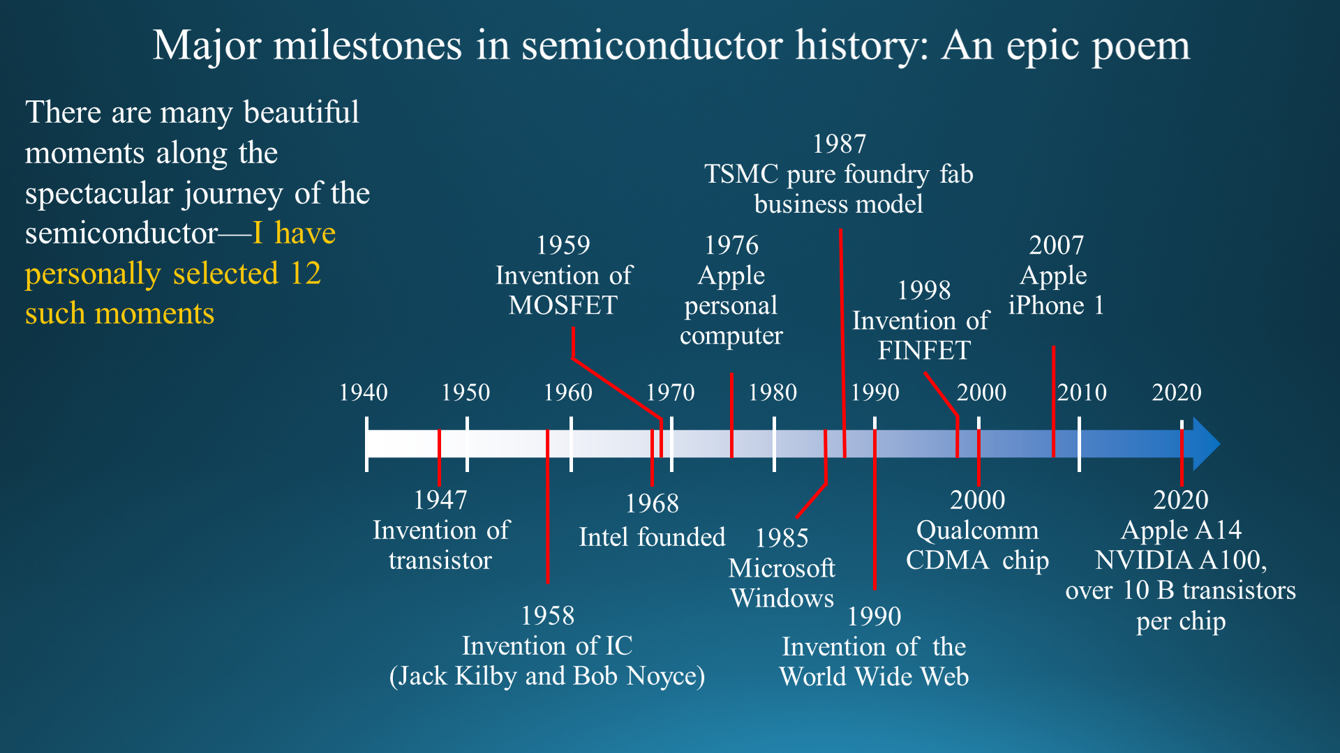
The development of the semiconductor world is vibrant, spectacular, magnificent, and epic, with countless beautiful chapters. I have identified twelve such chapters that I believe mark the major milestones along this journey: (1) the invention of the transistor (1947); (2) the invention of the IC (1958); (3) the invention of the MOSFET (Metal-Oxide-Semiconductor Field-Effective Transistor) (1959); (4) the founding of Intel (1968), which would eventually lead to Moore’s Law and the Wintel (a term for the partnership between Microsoft Windows and Intel’s CPU) personal computer architecture between 1968 to 2016; (5) the birth of Apple’s personal computer (1976); (6) the release of Microsoft’s Windows 1.0 (1985) and subsequent increased demand for transistors from Wintel personal computers; (7) TSMC’s pure semiconductor foundry business model (1987); (8) the invention of the World Wide Web (1990), connecting personal computers to the internet; (9) the invention of FINFET (Fin Field-Effect Transistor) (1998), transforming transistors from two dimensional to three dimensional structures, thereby extending Moore’s Law to technology nodes smaller than 20 nm; (10) Qualcomm’s CDMA (Code Division Multiple Access) telecommunication chip (2000), expanding the bandwidth of internet connections; (11) the birth of Apple’s iPhone 1 (2007); and (12) Apple’s A14 chip and NVIDIA’s A100 chip (2020), each chip containing more than 10 billion transistors. Below, I will discuss in detail two of the milestones that affected me the most—the birth of the iPhone 1 and TSMC’s pure semiconductor foundry business model.
Episode 1: the birth of the iPhone 1
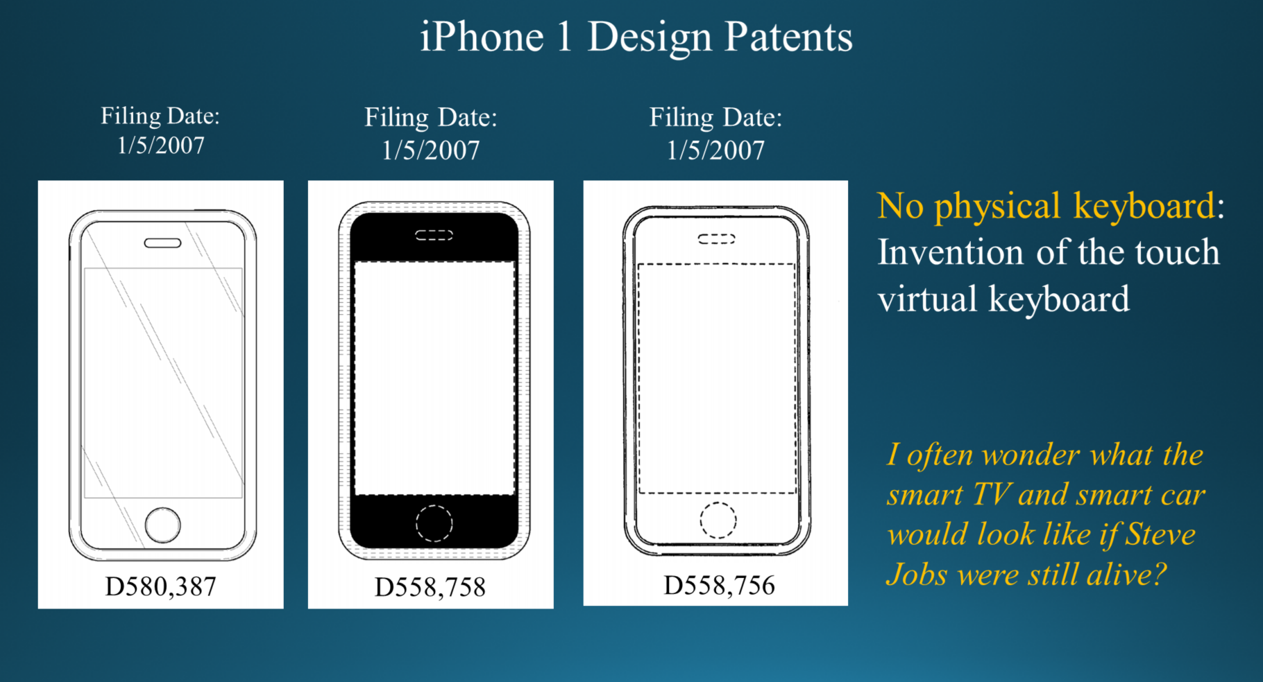
On January 5, 2007, Apple filed three U.S. design patent applications related to the iPhone on the same day. (Design patents, unlike the better known utility patents, contain only design figures and do not require any word descriptions.) The patents submitted by Steve Jobs and his co-inventors were unique in that they did not include an actual keyboard in the design of its mobile phone. Apple had launched a major invention in the history of technology: the virtual touch keyboard. Additionally, the four corners of the iPhone in the patents were designed as smooth curvatures instead of the right angles seen in other mobile phones. This made the iPhone more aesthetically pleasing to hold in your hand. (Jobs was an artist and an expert of living—I’ve often wondered what smart TVs and smart automobiles would look like if he were still alive today!) Ever since the release of the iPhone 1 in 2007, humankind’s lifestyle and society as we know it has been completely changed, and the general public finally became aware of the semiconductor’s importance to humanity.
For many years, I had been concerned and had been hoping that Harvard University would upgrade its Division of Engineering and Applied Sciences (DEAS) into being its own school. In 2007, the very same year of the iPhone’s release, Harvard, which has always been proud of its liberal arts and social sciences departments, finally recognized the impact of technology by officially establishing its School of Engineering and Applied Sciences (SEAS) in 2007.
It is noteworthy that Apple’s iPhone 1 combined telecommunications and computers, two industries previously irrelevant to each other, in a single device. This actually led to many infringement lawsuits of related patents and a wave of companies buying up telecommunication patents. In 2011, Apple, Microsoft, Sony, and Research in Motion (RIM) jointly purchased telecommunication patents from Canada’s Nortel Networks for 4.5 billion dollars. In 2012, Google bought Motorola Mobility for 12.5 billion dollars aiming for its telecommunication patents. This wave also led to the largest smart phone telecommunication chip company acquiring Megica, a company I had founded, in 2009, to deter potential patent infringement lawsuits from a computer CPU chip company because it had used Megica’s technology patents. (I will discuss this in further detail in Lesson 4).
Episode 2: TSMC’s pure semiconductor foundry business model
I am very lucky, honorable and grateful to have the opportunity in joining TSMC in its early days (1990-1997) and to have unforgettable experience in witnessing and participating in TSMC’s early pioneering and establishment of its pure semiconductor foundry business model. Under this approach, TSMC produced chip products designed by its customers, only providing customers with manufacturing services and not selling products under the TSMC name. In its pure foundry business model, TSMC cleverly and successfully implemented the concept of “Shared Capacity” in the semiconductor manufacturing. Interestingly, some of the most successful startup companies in recent years, such as Airbnb (shared lodging), Uber (shared ride), and WeWork (shared office), would come to adapt and build up this “Shared Capacity” business model as non-conventional and breakthrough methods of operations in their own respective industries.
TSMC's pure foundry model also has a unique advantage due to the concept of "shared process technology." The development and manufacturing of each process technology was tested and validated against numerous customer products. Not only is every customer's application different, their design styles also vary widely. The wide range of customers also function to refine each generation of TSMC's process technology by providing cases for comprehensive debugging and uncovering all potential weaknesses of the process technology. With each uncovered weakness, TSMC would perform failure-mode analysis to find failure causes, and improve their process technology or create new design rules based on the found causes, eventually allowing their technology to accommodate all different customers with a common process technology having wide process window, and resulting in high yield and low cost manufacturing.
To add value for manufacturing in the supply chain as a pure foundry company, TSMC developed in its early days a model cost-effective “Volume Production” technology, which deems a technology to have been successfully developed only when production volume surpasses 10,000 wafers per month with high yield and low cost; this model differs that for technologies producing small volume of 1, 10, or 1,000 wafers per month. Furthermore, TSMC pioneered the concept of applying very expensive wafer defect inspection equipment for in-line production monitoring at critical process steps since its early days. The very expensive wafer defect inspection equipment include KLA defect inspection machine, Scanning Electron Microscope (SEM) and etc. Most other IC manufacturing fabs then used these very expensive equipment only for failure-mode analysis on the finished defective IC wafers or chips. By doing so, TSMC’s wafer production is, analogously, not walking blindly in the dark, instead, they lighted up lamps, opened eyes along the way, and therefore, the wafers could safely arrive the finished point. The in-line production monitoring concept ends up with high-yield cost-effective wafer manufacturing.
TSMC’s success can be linked to core tenets found within the company’s name—“Taiwan Semiconductor Manufacturing Company” (TSMC)—emphasizing two of its major characteristics: “Taiwan” and “manufacturing”. In the early stages of its pure foundry business model, TSMC experienced skepticism from investors and even people within the semiconductor industry. This was due to the many hurdles presented by having chip design and manufacturing take place in two companies otherwise not affiliated with each other. For example, one major difficulty TSMC faced was figuring out how to develop new technology node processes without having any products of its own. Recounting my personal experiences, when participating in developing IBM’s first and second generation CMOS processes, we used IBM’s mainframe computer chip as the process development vehicle; when participating in the development of the multichip package (MCM) at AT&T Bell Labs, we used AT&T’s cross-point switching chip as the process development vehicle. Therefore, one might imagine how developing new processes without having our own products could be a major hurdle during this time period (1990 to 1995) when I was leading TSMC’s research development team.
Fortunately, and contrary to the prevailing sentiment at the time, TSMC’s pure semiconductor foundry model fostered business collaborations instead of competition with customers—they came to trust TSMC and treat its factories as their own. Such seamless partnership between chip design and manufacturing ended up being the perfect solution. On certain occasions, customers even transferred their most valuable technologies to TSMC at no cost for securing their planned production capacity. For example, when TSMC was developing the 0.8 µm process, VLSI technology Inc. (a company based in Silicon Valley) provided the process development test chip for TSMC to use at no cost. Even more worthy of mentioning is that in 1993, during which TSMC was developing the 0.5 µm process, AMD was very confident of the competitiveness of the 486 CPU chip it had designed using the 0.5 µm process but happened to lack production capacity. In need of TSMC’s 0.5 µm process production support, AMD transferred two sets of very valuable process modules, the Tungsten Plug and Chemical Mechanical Polishing technologies, to TSMC at no cost. Worldwide, only Intel and AMD (the two companies that produced the 486 CPU chip) had these two process modules at the time. With these two process modules in hand, it was as though TSMC’s 0.6 and 0.5 µm processes had taken a magic Dabu pill that provided a huge boost in the advancement of its technology. Unfortunately, the sales of AMD’s 486 CPU chip did not meet its lofty expectations, and orders did not spike as expected. As a result, while AMD’s 486 CPU chip was never produced at TSMC, TSMC benefited from obtaining the two valuable process modules. All throughout this technology transfer, there were frequent communications between the two companies. To this day, I can still remember AMD’s outsourcing managers, technology managers, and engineers vividly and do so with full gratitude. Surely enough, God was not blind, and AMD’s good conscience was finally paid off. After almost 30 years, AMD’s 7 nm and 5 nm CPU chips were finally produced at TSMC. AMD’s business thrived and flourished, becoming one of the leaders of the semiconductor industry. Additionally, when TSMC was developing its 0.35 µm process in 1994, it even spent millions of dollars to purchase Hewlett Packard’s 0.35 µm 64K SRAM designed product as the process development vehicle.
TSMC now possesses the world’s strongest computer-aided design (CAD) department, providing CAD Kits, Cell Library, and IP design services for chip designing companies and has also been providing advanced packaging manufacturing services since 2016. With addition of the strong design services and packaging manufacturing services in recent years along with the mask manufacturing and wafer testing services it has provided since the company’s establishment, TSMC now has established a solid, leading horizontal partnership business model for chip design and manufacturing functions being separated at two non-affiliated companies. This has allowed TSMC to overtake almost all of the vertically integrated device manufacturing (IDM) semiconductor companies. TSMC’s pure semiconductor foundry business model overturned the notion that “manufacturing” is of low value in the industry supply chain as countries worldwide now eagerly invest in the wafer manufacturing industry. TSMC’s pure semiconductor foundry business model can be viewed as a major revolution in the history of semiconductors. TSMC became the world’s highest valued semiconductor company in 2020 and has been integral to Taiwan’s standing in international relations.
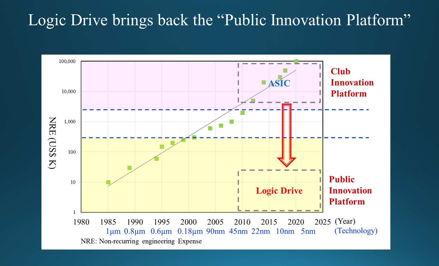
Another reason that TSMC was able to succeed with its pure semiconductor foundry business model early on can be credited to the provision of a “Public Innovation Platform”. When I was working at TSMC between 1990 to 1997, a creative and talented IC designer could found an IC design company with just hundreds of thousands or one to two million dollars and use TSMC’s 1 to 0.35 µm manufacturing processes to realize their design creations. Many of today’s IC design companies, such as NVIDIA, Qualcomm, Broadcom, Marvel, Realtek, and hundreds and thousands of others all started this way back then. It was a time when heroic and ambitious upstarts flourished, eagerly trying to make a mark. While some rose to the top, becoming industry leaders and the kings and champions of the era, many others certainly also lost everything and quietly bowed out. These startup companies would come to defeat the world’s vertical IDM semiconductor industry giants and, more importantly, brought about the birth of the life-changing iPhone 1 in 2007, which used many of the chips designed by startup IC design companies and manufactured by TSMC. You could say that TSMC was, in fact, the hero behind the scenes in the story of the iPhone 1. However, one could argue that TSMC no longer maintains the early ideals of its “Public Innovation Platform” today, now resembling more of a “Club Innovation Platform”. Case in point, even a set of 10 nm masks now costs about three million dollars, and roughly nine million dollars for 7 nm masks. The non-recurring-engineering (NRE) expense for developing a 7 nm chip is in the tens or hundreds of millions of dollars. Only system companies like Apple or major IC design companies like Qualcomm, MediaTek, NVIDA and AMD have the resources to participate and buy into the astronomically expensive game of the 7 nm advance manufacturing process.
iCometrue’s proposed “Logic Drive” to help bring back the “Public Innovation Platform”
In order to let more people afford to participate in innovation, I believe that we must provide an alternative for creative chip designers with limited funding. In 2016, I proposed the prospect and dream of such a solution: the “Logic Drive”. With the Logic Drive, several hundreds of thousands to a few million dollars would be enough to establish an IC design company that could utilize TSMC’s cutting edge 10 nm or more advanced technology node process to realize their innovations—in other words, providing a way for 99% of the general public to participate in the game of the wealthy 1%. The idea behind the Logic Drive is to use software to configure and re-configure the hardware circuits, using standard commodity FPGA (Field Programmable Gate Array) IC chips or chiplets.
The main concepts behind the Logic Drive are fourfold: (1) Using technology more advanced than 10 nm, the standard commodity FPGA IC chip or chiplet in the Logic Drive would contain a sufficient number of transistors and provide fast processing speed with low power consumption; (2) Standardizing FPGA IC chips and designing and converting them into a commodity like DRAM would allow the standard commodity FPGA IC chip or chiplet to become cheap; (3) Packing multiple standard commodity FPGA IC chips into an advanced multi-chip package, the number of transistors would be greatly increased; (4) The brain-like elasticity and integrality of the FPGA IC chip would likely inspire new ground-breaking architectures and algorithms, especially in artificial intelligence and machine learning, such as the CGRA (coarse grained reconfigurable array). As a result, the price and power consumption of the FPGA IC chip will decrease significantly while its speed and function will see considerable improvements.
In addition, iCometrue proposed to add a non-volatile flash memory IC chip into the advanced package to store the programming codes for configuring the logic circuits of the FPGA IC chip. This turns the FPGA IC chip within the Logic Drive into a non-volatile element and the Logic Drive can be used as an ASIC chip. Smart and creative IC designers would be able to purchase the Logic Drive and use software to configure the hardware circuits of FPGA IC chips that use the most advanced process technology, allowing the realization of their ideas at a lower, attainable cost. Furthermore, the hardware circuits of the FPGA IC chip in the Logic Drive can be re-configured by software for a new computing logic, and the re-configuration data is stored in the non-volatile flash memory chip packaged in the same Logic Drive. The Logic Drive is now like the Solid-State Drive or Solid-State Disk (SSD); the only difference is that SSD is for storing data memory, while logic drive is for storing computing logic.
While being transformed into a “Club Innovation Platform” in its technology nodes more advanced than 10 nm, TSMC has the opportunity to re-establish its “Public Innovation Platform” for talent IC designers by allocating a portion of its 10 nm or more advanced technology production capacity to manufacturing standard commodity FPGA IC chiplets for the Logic Drive. Then, the previously excluded 99% of innovative IC designers would be able to also participate in using the 10 nm or more advanced technology process. This would enhance TSMC’s pure semiconductor foundry business model and help TSMC in sustaining its long-lasting success.
(This article was translated from the article (in Chinese) published in “DIGITIMES” on November 17th, 2021, while with some revisions.)
Link of “DIGITIMES”: Lesson 3