If you have comments, questions or interest described in the following article, please contact us at:
Email: cometrue@icometrue.com
Lesson 2: The magical lithography machine: playing games with wavelengths
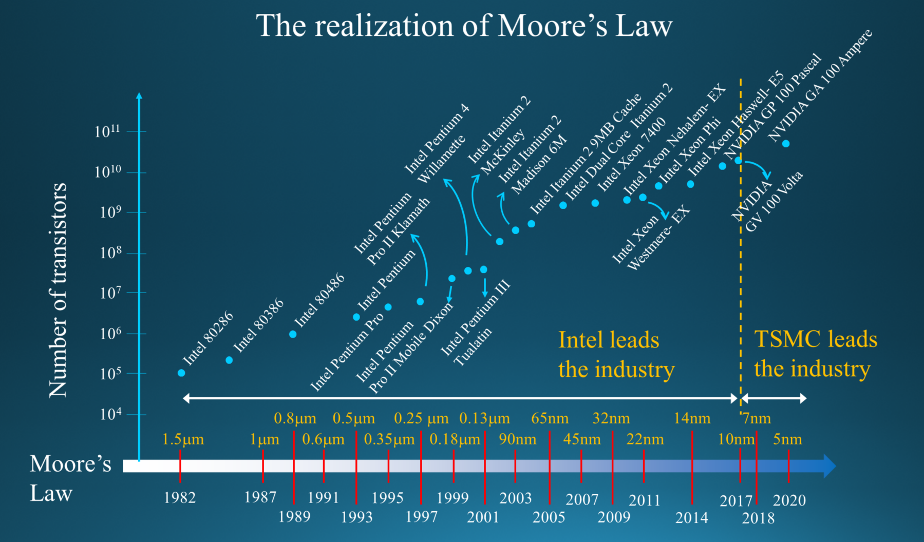
The minimum width of the IC circuit is roughly the same as the wavelength of the light source used by lithography machines; as a result, the progression of Moore’s Law was determined by the wavelength of the light source: (1) Between 1984 to 1990, the 436 nm ultra-violet (UV) light G-line generated by mercury lamps defined the 1.5 to 0.8 µm technology node processes; (2) between 1991 to 1996, the 365 nm UV light I-line generated by mercury lamps defined the 0.6 to 0.35 µm technology node processes; (3) between 1997 to 2001, the 248 nm deep UV (DUV) light generated by KrF laser defined the 0.25 to 0.13 µm technology node processes; (4) between 2002 to 2019, the 193 nm deep UV (DUV) light generated by ArF laser defined the 90 to 7 nm technology node processes; and (5) since 2019, the 13.5 nm extreme UV (EUV) light generated by tin ions excited by CO2 laser defined the 7, 5, and 3 nm technology node processes. In line with Moore’s Law, the number of transistors in an IC chip doubled approximately every 20 months (i.e., the area size of transistors halved), and the linear dimension of transistors reduced to approximately 70% with each generation of semiconductor process, producing the well-known 0.5 µm, 0.35 µm, 0.25 µm, 0.18 µm, 0.13 µm, 90 nm, 60 nm, 40 nm, 28 nm, 20 nm, 14 nm, 10 nm, 7 nm, 5 nm, 3 nm, and 2 nm technology nodes.
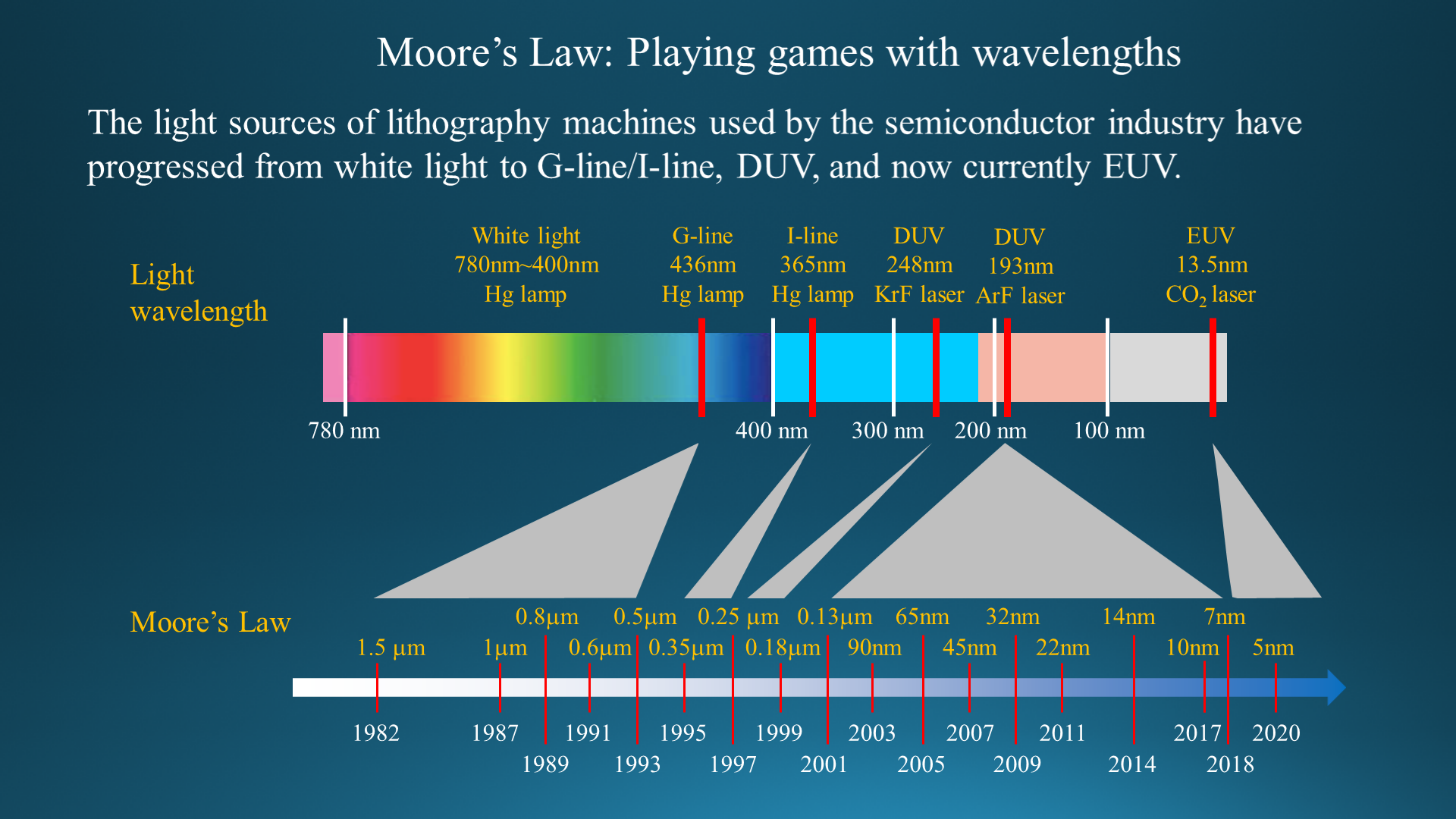
After the debut of the 193 nm DUV light source was mature for volume production in 2002, mankind struggled to develop technologies that could provide lithography machines with light sources of shorter wavelengths. It was not until 2019 that the technology for producing a stable 13.5 nm EUV light source was finally developed and used for volume production. During those seventeen long years while the world awaited a shorter wavelength light source, Taiwan Semiconductor Manufacturing Company (TSMC) was able to continue advancing technologically, challenging the physical limitations of light waves and managing to successfully extend the application of the 193 nm DUV to manufacture 7 nm technology node products. This achievement could only have been made possible through the hard work, strong determination and strict manufacturing discipline TSMC poured into this endeavor, reflected in its culture and technological ingenuity. It is a story that demonstrates how diligence compensates for limitations in nature.
From a cultural perspective, TSMC pioneered a research and development system operating under a 24-hour, three work shifts schedule to reduce the cycle time of Moore’s law. In many ways, Taiwan’s densely-packed urban environment and “motorcycle culture” is ingrained in its people, bringing about a mindset of flexibility and an innate desire to squeeze as much as possible out of limited resources—this contributed to TSMC’s focus on continuous and incremental improvement during this time. Looking back on this period between 1990 to 1995 when I led TSMC’s R&D, it should be noted that TSMC did not fully follow Moore’s Law in developing a new generation of process technology but instead gradually and incrementally developed eight generations (0.8, 0.7, 0.65, 0.6, 0.55, 0.5, 0.45, and 0.35 µm) of process technologies, catching up to the rate of Moore’s Law one small step at a time. In addition, TSMC continuously re-used process modules and materials of previous generations of technology nodes until they were completely unusable and had to be replaced with new ones.
In terms of its technology, through its hard work, endurance, perseverance, and strong engineering and manufacturing management ability, TSMC applied complicated technological processes, such as immersion exposure, phase-shift mask, and multiple exposures to eventually succeed in using 193 nm DUV to mass-produce 10 nm and 7 nm technology node IC products. As a result, TSMC was in position to continue its development of advanced technology nodes using EUV to mass-produce 7 nm and 5 nm technology node IC products once the EUV lithography technology was mature and reliable enough for application. Intel, in comparison, was not so successful in using 193 nm DUV to develop a process for mass-producing 10 nm technology node IC products and found itself stuck in a position where it was neither able to advance nor retreat.
It was due to this divergence that TSMC eventually replaced Intel’s dominance and assumed leadership in the semiconductor manufacturing industry. The pathways and factors of how TSMC came to surpass Intel as I have described above are based on my personal view and understanding. On March 24, 2021, Intel’s new CEO Pat Gelsinger made similar comments during his speech “Intel Unleashed: Engineering the Future” webcast, acknowledging, “When Intel initially designed 7 nanometers, EUV was still a nascent technology, so we developed our process to limit the use of EUV. But this also increased the process complexity. As EUV then matured and became more reliable, we experienced the domino effects of our 10-nanometer delay which pushed out 7-nanometers and ultimately put us on the wrong side of the EUV maturity curve.”
When recounting this story, it is impossible not to mention the engineering masterpiece that is the EUV lithography machine. An EUV light source is generated much in the same manner in which a star generates light violently using energy from extremely high temperature and heat. The process begins with using a CO2 laser to strike droplets of tin (50 thousand drops per second), causing the droplets to evaporate into gas and be converted to plasma (Laser Produced Plasma, LPP). When the temperature of the plasma reaches 4x10⁵ºC (30 eV), its energy will excite the tin atom into forming multicharged ion (Sn+8 –Sn+19) at an excited state with very high energy. At this high energy state, when a multicharged ion interacts with an electron and returns to a lower energy state ion or atom, it will generate EUV. An EUV lithography machine with an output power of 250 Watts requires an input of 1.25 MW power (0.02% conversion rate) and consumes 30 MWHs of electricity each workday—equivalent to three thousand times the electricity an average household consumes in a day. Advancements in EUV technology have greatly impacted human civilization and have the potential of being awarded the Nobel Prize in the future.
With the development of the EUV lithography machine and three-dimensional transistors—including the mass production of fin field effect transistors (FinFET) and the developing gate-all-around field effect transistor (GAAFET)—Moore’s Law foretells continued progress with no end in sight in the near future.
The first man-made “sun,” EUV lithography, is already in volume production now—it is very fascinating and exciting to now witness the metaphorical rise of yet another new man-made sun. In recent years, MIT’s Commonwealth Fusion Systems (CFS) has achieved major advances in fusion energy. The EUV machine uses a CO2 laser to excite tin drops in a localized region around the laser beam focus in a chamber and to produce extremely hot plasma of tin ions for generating EUV light, so that the extremely hot (4x10⁵ºC) plasma of tin ions are kept isolated and far from the chamber walls. In similar fashion, CFS uses very high magnetic fields to confine and localize extremely hot (1x10⁸ºC) plasma of protons and electrons for igniting nuclear fusion reactions while keeping them isolated and far from the chamber walls. If MIT’s CFS could be inspired and encouraged by the success of the EUV machine to successfully produce huge amounts of nuclear fusion energy, human civilization will be thoroughly revolutionized by these two man-made suns.
(This article was translated from the article (in Chinese) published in “DIGITIMES” on November 16th, 2021, while with some revisions.)
Link of “DIGITIMES”: Lesson 2